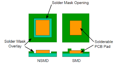
Two types of PCB solder mask openings commonly used for surface mount leadless style packages are:
1. Non Solder Masked Defined (NSMD)
2. Solder Masked Defined (SMD)
As their titles describe, the NSMD contact pads have the solder mask pulled away from the solderable metallization, while the SMD pads have the solder mask over the edge of the metallization, as shown above. With the SMD Pads, the solder mask restricts the flow of solder paste on the top of the metallization which prevents the solder from flowing along the side of the metal pad. This is different from the NSMD configuration where the solder will flow around both the top and the sides of the metallization.
Typically, the NSMD pads are preferred over the SMD configuration since defining the location and size of the copper pad is easier to control than the solder mask. This is based on the fact that the copper etching process is capable of a tighter tolerance than the solder masking process. This also allows for visual inspection of solder fillet.
In addition, the SMD pads will inherently create a stress concentration point where the solder wets to the pad on top of the lead. This stress concentration point is reduced when the solder is allowed to flow down the sides of the leads in the NSMD configuration.

No comments:
Post a Comment