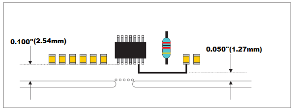
1. Traces and vias should be a minimum of 0.050"(1.27 mm) away from routed/scored edge.
2. Components should be a minimum of 0.100"(2.54 mm) away from routed/scored edge.
These rules are to help prevent components or board damage during the depaneling process and prevent flooding during the wave soldering process.
For 0.062" (1.6 mm thickness) Printed Circuit Boards:
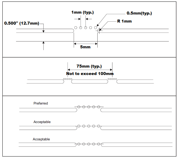
1. Perforation holes should be typically spaced at 1 mm intervals.
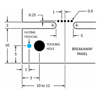
2. Tab routed with 1 mm radius.
3. Routed slot should be 2 mm minimum, for single image panels. Use 3 mm routed slots when two or more boards are in a panel. This allows for more accurate edge dimensions.
4. 75 mm typical distance between tabs, not to exceed 100 mm.
5. Place tabs approximately 25 mm from corners to reduce sagging during reflow or wave soldering.
6. Desirable to have at least one tab per side.
7. Slight inset of perforation is preferred; it provides an edge which requires little or no additional labor to clean up.
NOTE: Two parallel edges are required for a PCB to be processed in the SMT line. This is to prevent skewing through the conveyor system. All odd shaped PCB's MUST have edge rails incorporated to meet this requirement. Custom reflow fixtures will be made if this requirement is not met.


No comments:
Post a Comment