
Monday 10 December 2018
Friday 7 December 2018
Altium Designer : Creating Logo

To Import Logo to silk screen, create logo in MS Word. Copy and paste in Altium.
Thursday 6 December 2018


Wednesday 5 December 2018
Tuesday 4 December 2018

Monday 3 December 2018
Altium Designer : Creating Custom Board Outline and Keepout Area
It is a good design practice to add keepout area along the board outline. Recommended keep out line thickness is 20 mil.
Friday 23 November 2018
Altium Designer: Useful Shortcuts for Component Placement
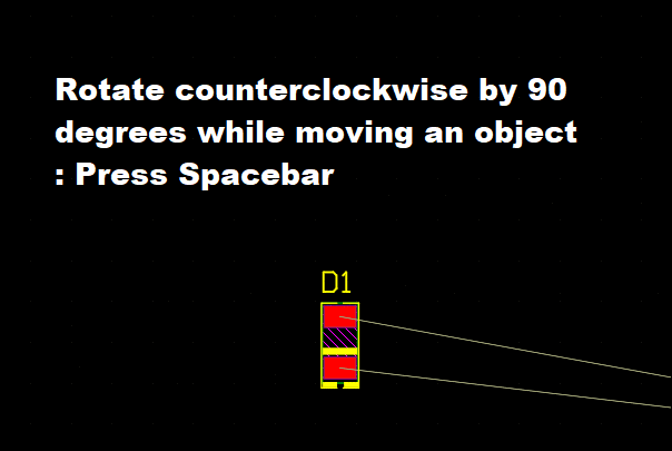
- Rotate counterclockwise by 90 degrees while moving an object : SPACEBAR
- Align selected objects by top edges : SHIFT + CTRL + T
- Distribute selected objects equally in horizontal plane : SHIFT + CTRL + H
- Align selected objects by left edges : SHIFT + CTRL + L
- Align selected objects by right edges : SHIFT + CTRL + R
- Distribute selected objects equally in vertical plane : SHIFT + CTRL + V
- Align selected objects to grid : SHIFT + CTRL + D
- Align selected objects by bottom edges : SHIFT + CTRL + B
Thursday 22 November 2018
Altium Designer : Pcb Panelization
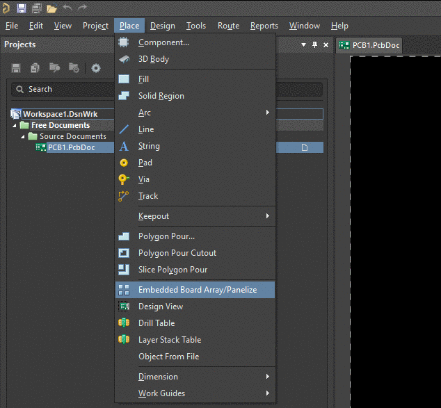
On the Place tab, Select Embedded Board Array/ Panelize. Click anywhere in the PCB area. Under Properties menu, select your PCB and set desired Column margin and Row spacing.
Altium Designer : Creating Board Outline From Mechanical Outline and Making Cutout Holes
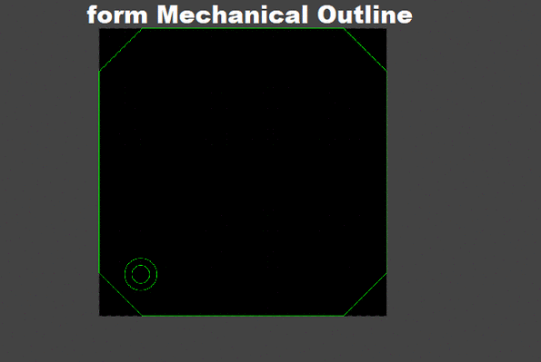
Select Mechanical Outline. Under Properties menu, Change Mechanical outline layer to user defined board outline layer.
To create custom board shape, select board outline that has been created. On the Design Tab, in the board shape, select Define from selected Objects.
To create a cutout hole, select the desired outline. On the Tool Tab, in the Convert, select Create Boardcutout from selected primitives.
Altium Designer : Moving Design Origin to User's Preferred Location
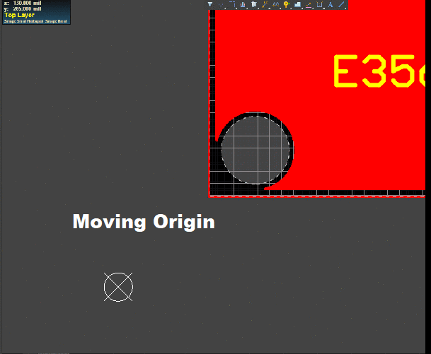
On the Edit tap, in the Origin, choose Set.
Altium Designer, Shortcuts for Viewing, Changing Grid and Snap Setting

Toggle measurement Unit : Q
Accessing Grid menu : G
Changing snap setting : SHIFT + E
Switching 2D and 3 D View : 2 & 3
Fit all objects into view : CTRL + PAGE DOWN
Zoom in around cursor (zooms around cursor, position the cursor first) : CTRL + Mouse-wheel up (or PAGE UP)
Zoom out : CTRL + Mouse-wheel down (or PAGE DOWN)
Wednesday 21 November 2018
AAA Battery Protection with Wrong Polarity LED Indicator

Thursday 7 June 2018
A Basic Transistor Amplifier with self-bias
Wednesday 6 June 2018
Common Mode and Differential Mode Filters to limit EMI Issues

Thursday 24 May 2018
Simple Logic Gates using Diodes

Diodes can be used for implementing simple logic gates such as AND or OR combinations. For AND gate, all inputs must be tie to high, 5V for the output logic high. For OR gate, the output is high if any input(s) are high.
Thursday 10 May 2018
Emergency Phone Charger From 3 x AA Battery with output Protection

Three AA batteries (3 x 1.5V) is using as emergency power source for mobile device or phone charging. Output current is limited to 0.5A and protected from out short circuit or high current drawn from the batteries.
Saturday 21 April 2018
Guidelines for the design and layout of high-speed digital logic PCBs
- Give a lot of consideration to component placement and orientation
- Avoid overlapping clock harmonics. Make harmonic table for each clock
- Clock signal loop area must be kept as small as possible. Get paranoid about clocks.
- Use multilayer boards with power and ground planes whenever possible.
- All high frequency signal traces must be on layers adjacent to a plane
- Keep signal layers as close to the adjacent plane layer as possible (<10 mils)
- Above 25MHz PCBs should have two or more ground planes
- When power and ground planes are on adjacent layers, the power plane should be recessed from the edge of the ground plane by a distance equal to 20 times the spacing between the planes
- Bury clock signals between power and ground planes whenever possible.
- Avoid slot in ground plane. Also applies to power plane.
- If a segmented power plane is necessary, signal traces must not be routed over the slots.
- Filter (series terminate) the output of clock drivers to slow down their rise/fall times and to reduce ringing typically 33 to 70 ohms
- Place the clock & high speed circuitry as far away from I/O area as possible.
- Use a minimum of two equal values decoupling capacitor on DIP packages, four on square packages. On high frequency/ high power/noisy IC many more capacitors may be necessary
- Consider using embedded capacitance PCB structure for decoupling on h-f boards (>50 MHz)
- Use impedance-controlled PCB layout technique with proper terminations where necessary
- On impedance-controlled PCB, do not transitions the signal from one layer to another unless both layers are referenced to the same plane
- On non-impedance-controlled PCBs, when a clock transitions from one layer to another & the layers are referenced to different planes add a transfer via or capacitor between the planes
- All traces whose length (in inches) is equal to or greater than the signal rise/fall time (in nanoseconds) must have provision for a series-termination resistor (typically 33 ohms)
- Simulate all nets whose length (in inches) is equal to or greater than the signal rise/fall time (in ns)
- Connect logic ground to the chassis (with a very low Z connection) in the I/O area. This is crucial!
- Provide for an additional ground to chassis connection at the clock/oscillator location.
- Additional ground to chassis connection may also be required
- Daughter boards (with h-f, noisy devices and/or external cables) must be properly grounded to the motherboard and/or chassis (do not rely the ground pin s in the connector to provide this ground)
- Provide C-M filters on all I/O lines. Group all I/O lines together in a designated I/O area of PCB
- Shunt capacitors used in I/O filters must have a very low impedance connection to chassis.
- Use a power entry filter on the dc power line (both C-M and D-M)
- Most products in plastic enclosures need to be provided with an additional metal reference plane
- Consider the use of board level component shields where applicable
- Ground all heat sinks
Tuesday 17 April 2018
Bypass & Decoupling Caps Selection for Voltage Regulators

The main function of the bypass capacitor is to create an AC shunt to remove undesirable energy from entering susceptible areas. The bypass capacitor is acting as a high frequency bypass source to reduce the transient circuit demand on the power supply unit. Usually, aluminium or tantalum capacitor is a good choice for bypass capacitors, its value depends on the transient current demand on the PCB, but it is usually in the range of 10 to 47 uF. Larger values are required on the PCB with a large number of integrated circuits, fast switching circuits, and PSUs and having long leads to PCB.
Decoupling Capacitors
During active device switching, the high frequency switching noise created is distributed along the power supply lines. The main function of the decoupling is to provide localised source of DC power for the active devices, thus reducing switching noise propagating across the board and decoupling the noise to ground.
Ideally, the bypass and decoupling should be placed as close as possible to the power supply inlet to help filter high frequency noises. The value of decouupling capacitor is approximately 1/100 or 1/1000 of the bypass capacitor. For better EMC performance, decoupling capacitors should be placed as close as possible to each IC, because trace impedance will reduce the effectiveness of decoupling function.
Creamic capacitors are usually selected for decoupling; choosing the value depends on the rise and fall times of the fastest signal. For example, with a 33 MHz clock frequency, use 4.7nF to 100nF, with a 100 MHz clock frequency use 10nF.
Apart from the capacitance value when choosing the decoupling capacitor, the low ESR of the capacitor also affects its decoupling capabilities. For decoupling, it is preferable to choose capacitors with a ESR value less than 1 ohm.
Thursday 12 April 2018
Logic Inverter with Schmitt Trigger
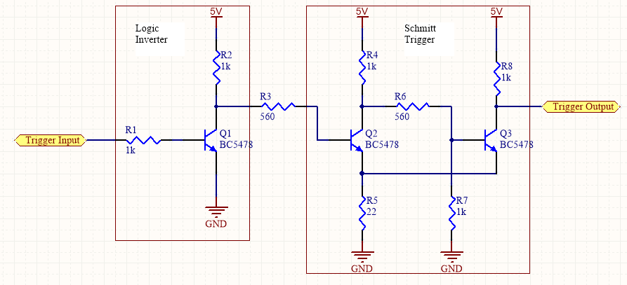
This circuit can take noisy active low input signal, invert the logic and provide clean Schmitt Trigger output.
Wednesday 11 April 2018
Soft-Start and Protection Circuit

When the input is below 18 V, Q1 is OFF state allowing C3 to be charged though R3. Thus turning on Q105. Once the input voltage exceed 18 plus two diode drop Volts, Q1 will turn on that discharge C3 and Q105 is OFF.
Once the input goes back below 18 V, Q1 is turn off again. This allows C3 to be charged slowly resulting soft-start at the output.
Tuesday 10 April 2018
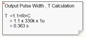
Pulse Width Stretcher using 555 Timer IC

This circuit will invert and stretch the short period active low input signal as below.

Required pulse width can be calculated by using this equation.
Monday 9 April 2018
Micro-controller Output Protection by Current Limiting

Maximum current = VBE,Q1A / R2 = 0.65 / 33 = 19.7 mA
Sunday 8 April 2018
High Voltage Monitoring/ Measuring using Microcontroller's ADC input

Voltage divider resistor network is used to step monitored voltage down to the range as necessary for A/D conversion. Passive low-pass filter is used for noise rejection.
Saturday 7 April 2018
Voltage Doubler Circuit

Reverse Polarity Protection
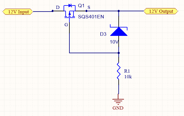
Zener Voltage = 10 V, Q1-VGS max = +/- 20V
Zener diode, D3 will protect the gate from excessive voltages/ unwanted spikes
By
referring the Gate signal to the ground line, the device is fully turned on when the
battery is applied in the right polarity. For the first start up, the intrinsic body diode
of the MOSFET will conduct, until the channel is switched on in parallel. The Zener
diode will clamp the Gate of the MOSFET to its Zener voltage and protecting it
against overvoltage.
By reverse polarity, the MOSFET will be switched off, because the Gate Source
voltage for this case will be positive (voltage drop over the Zener diode).
Friday 6 April 2018
Logic Input/ Push Button input Buffer Circuit

This circuit squares up and debounces a push button or logic input signal.
Bi-directional Logic Level Shifter
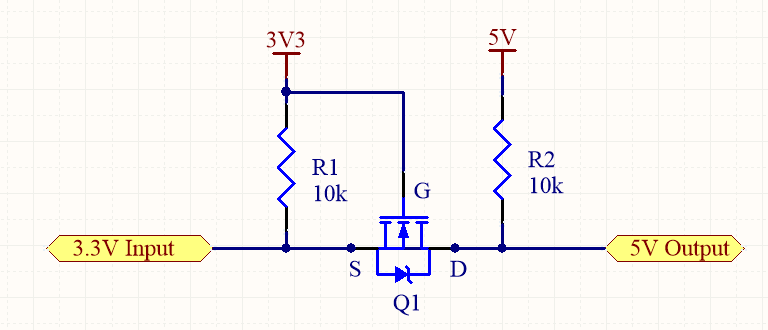
Input = 0V ; VGS > VGS(th) ; FET = ON ; Output = 0V
Input = 3.3V ; VGS < VGS(th) ; FET = OFF ; Output = 5V
Thursday 5 April 2018
Protecting microcontroller's Inputs
1) Filtering
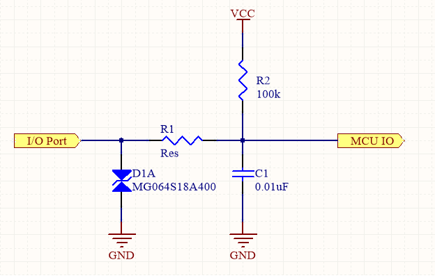
This circuit can be used to protect I/Os of micro-controller/ processors. D1A is used for Transient Voltage Suppression or ESD protection. R1 acts as current limiting resister as well as low pass filter together with C1. The value of the resistor and the capacitor must be sized so that the micro-controller does not miss any signals.
Rise time of the fastest income edge = 2.2 RC
2) Limiting Current

This circuit limit the input current to 23.2 mA (VZ/R1 = 5.1 / 220).
3) Limiting Voltage

Use schottky diodes with 0.2 Vf for better performance. Once the voltage at I/O pin is greater than VCC by about 0.2V, the top diode will start to conduct. The bottom diode will conduct for voltage less than -0.2V.
Subscribe to:
Posts (Atom)