1) Artwork Printing:
Print your artwork on a transparent sheet.2) Exposing:
Kinsten Presensitized PCB is using for this prototype as it is low cost and easy to work. Remove light-proof protective film and expose the board in the Kinsten UV exposure box for 90 seconds.Align the artwork with the PCB inside the vacuum clamp, leave it inside the exposure box for about 5 minutes.
3) Developing:
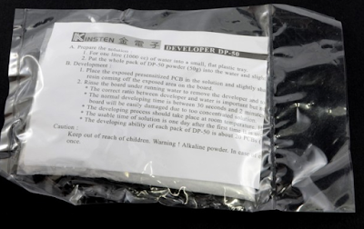
A sachet of DP-50 developer is mixed with 1 liter of 25°C water in a plastic container. The exposed PCB is gently agitated in solution. The exposed areas of resist will dissolve into the solution, leaving the green resist in areas that were not exposed to UV light as below.4) Etching:
Etching copper is done in the Kinsten Etching Tank for 4 to 10 minutes. Pour enough etching solution (Ferric Chloride or Ammonium Persulphate) into the tank and immerse the board. Use the air pump to allow the etchant to be bubble agitated until the unwanted copper foil etched away, only the circuit patterns left. Rinse the board with plenty of water.Remember “Safety First” always wear rubber gloves and protective eyewear when working with this etching compound. Kindly take note, once you've etched your board, the leftover solution should not pour it down the drain (legally). Take it to a hazardous waste facility.
Here is the final outcome. To get better results, make PCB trace thickness at least 10 or 12 mil and leave the wider gap between trace and GND copper pour.


No comments:
Post a Comment